Spiny Photovoltaics
April 18, 2012
Aside from optimizing the
photovoltaic material, itself, it's important that
photovoltaic cells take advantage of all the
insolation provided to them. In the case of flat panels, this often involves a motorized stage to
track the sun. Even then, the
refractive index difference between
air and the material will cause some of the light to be lost through
reflection.
One method of mitigating reflection is through the use of an
antireflection coating. Putting a layer of an
intermediate refractive index between your material (n = 3.96 for
silicon at
visible wavelengths) and air (n
o = 1.00) will help. The optimum refractive index of this coating would be √(n ⋅ n
o), which is about 2.00 for the silicon/air interface; but this trick will work for just a narrow range of wavelengths, and
sunlight is
broadband. That's why there have been many schemes to "trap" light in topographic structures.
In a
recent article (Solar Whispers, February 22, 2012), I reported on a light-trapping approach developed by a team of
Stanford University engineers. This involved hollow microspheres of
nanocrystalline-silicon on the surface of photovoltaic cells. These nanoshells support the
optical whispering gallery resonant modes that trap light to increase
efficiency. Other approaches involve regular arrays of silicon
nanowires on flat substrates that increase the path length of incident light by as much as seventy-three times.[1]
A team of
materials scientists from the
Swiss Federal Laboratories for Materials Science and Technology (EMPA) and the
Institut Européen des Membranes at the
Université Montpellier (France) has just published details of a light-trapping architecture for
zinc oxide (ZnO) nanowire solar cells that's based on the spiny structure of the
sea urchin.[2]
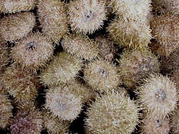
The green sea urchin (Strongheart droebachiensis).
(NOAA image))
This is a follow-up to these authors' previous research in this area. Their previously published results on ZnO nanowires,
electrodeposited onto surface-activated
polymer spheres, showed a twofold improvement of
light absorption compared to simple nanowire arrays; but these nanostructures had limited
mechanical stability.[2] In the present work, they hollowed-out the spheres and produced a photovoltaic structure by a low-cost and scalable process that allows a fine tuning of the optical absorptive properties.
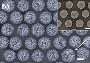
Ordered arrays of polystyrene spheres with ZnO nanowires. The scale bars are 2 μm.
(Fig. 2(b) of ref. 3, via arXiv Preprint Server).[3)]
The process starts with an array of
polystyrene spheres
self-organized into an array on a
fluorine-doped
tin oxide (FTO) coated
glass substrate. These spheres are reduced in size by
reactive ion etching, coated with ZnO using
atomic layer deposition (ALD), and then overlaid with a forest of ZnO nanowires, as seen in the above figure. The detailed process steps are as follow:[3]
a) An ordered monolayer of polystyrene microspheres is deposited on an FTO covered glass substrate by dip coating.
b) The size of the spheres is reduced using reactive ion etching with an oxygen plasma. The final size of the spheres is controlled by the etching time.
c) A conformal layer of ZnO, about 20 nm, is deposited on the spheres using ALD.
d) n-type ZnO nanowires of controlled length and diameter are electrodeposited on the thin ZnO layer.
e) The polystyrene spheres are dissolved in toluene, leaving hollow ZnO spheres studded with nanowires.
f) The nanowires are coated by electrodeposition with an absorber film of cadmium selenide (CdSe).
g) The assemblage is covered with p-type CuSCN by chemical impregnation.
h) A final gold electrode is formed by physical vapor deposition.
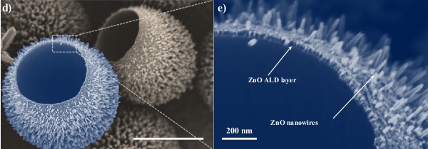
Hollowed polystyrene spheres with ZnO nanowires. These spherical shells were uprooted from the substrate by scratching to reveal the underside. The scale bar is 2 μm in the leftmost micrograph.(Figs. 2(d) and 2(e) of ref. 3, via arXiv Preprint Server).[3)]
These sea urchin inspired photovoltaics had a uniform absorption of up to 90% in the wavelength range of 400-800 nm. Solar conversion efficiencies of about 1.33% were achieved, which is less than that for published results for standard process ZnO/CdSe/CuSCN solar-cells (about 2%). The authors note that the process has the potential for optimization and improvement, and it might be applied to other materials.
Support for this research was from the
Swiss Federal Office for Energy, Solar Cell project, No. 103296.
References:
- Erik Garnett and Peidong Yang, "Light Trapping in Silicon Nanowire Solar Cells," Nano Letters, vol. 10, no. 3 (March 10, 2010), pp. 1082-1087; available as a PDF file, here.
- Jamil Elias, Claude Lévy-Clément, Mikhael Bechelany, Johann Michler, Guillaume-Yangshu Wang, Zhao Wang and Laetitia Philippe, "Hollow Urchin-like ZnO thin Films by Electrochemical Deposition," Adv. Mater. vol. 22, no. 14 (April 12, 2010), pp. 1607-1612.
- Jamil Elias, Mikhael Bechelany, Ivo Utke, Rolf Erni, Davood Hosseini, Johann Michler and Laetitia Philippe, "Urchin-inspired zinc oxide as building blocks for nanostructured solar cells," ArXiv Preprint Server, April 12, 2012).
Permanent Link to this article
Linked Keywords: Photovoltaic material; photovoltaic cells; insolation; solar tracker; refractive index; air; reflection; antireflection coating; silicon; visible light; wavelength; sunlight; electromagnetic spectrum; broadband; Stanford University; engineer; nanocrystalline-silicon; optical; whispering gallery; resonance; resonant mode; energy conversion efficiency; nanowire; materials scientist; Swiss Federal Laboratories for Materials Science and Technology; Institut Européen des Membranes; Université Montpellier (France); zinc oxide; sea urchin; green sea urchin; NOAA; electroplating; electrodeposition; polymer; sphere; light absorption; mechanical; arXiv Preprint Server; polystyrene; self-organized; fluorine; tin oxide; glass; reactive ion etching; atomic layer deposition; dip coating; oxygen; plasma; conformal layer; n-type; toluene; cadmium selenide; p-type; copper; Cu; thiocyanate; SCN; chemical impregnation; gold; electrode; physical vapor deposition; Swiss Federal Office for Energy.