Vacuum Tube Redux
August 9, 2011
The
transistor and I were born at about the same time, at the end of 1947. Useful and inexpensive transistors weren't available until many years thereafter, so it's no surprise that the first
electronic circuits I built used
vacuum tubes. I was aided in my electronics education by two neighbors, one of whom was a civilian
electronics technician for the
US Air Force. He repaired
television sets in his home as a side job, and he gave me many old television sets that I harvested for tubes and components.
The other neighbor was an
electrical engineer who worked at a military electronics division of
General Electric. He was also an
amateur radio operator, and "hams," as they are called, are always good at proselytizing their craft. Living in between these two, I got useful hardware from the North side of my house, and useful knowledge from the South side.
It took some time for transistors to displace vacuum tubes, especially in certain applications. Early transistors had very low
gain, and they were suitable just for
low power applications. They were
temperature sensitive to the point that they wouldn't work at all at what would be considered modest temperatures today. The first transistors were also
current amplifiers, not
transconductance amplifiers like vacuum tubes, which led to other application problems.
It was therefore no surprise, at least to those engineers who worked with both vacuum tubes and transistors, that the
Mikoyan-Gurevich MiG-25, a very successful
Soviet fighter aircraft that saw first active duty in 1970, was found to have most of its
avionics implemented with vacuum tubes. It's powerful
radar system had a
transmitter capable of sending radar pulses of about half a
megawatt! The MIG-25 was produced through 1984.
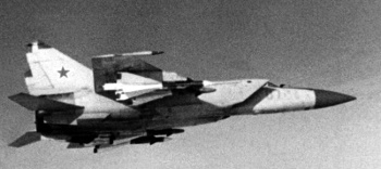
A Soviet MiG-25 interceptor aircraft armed with four AA-6 Acrid air-to-air missiles.
(Via Wikimedia Commons))
Eventually, transistors were developed with better properties, and they were sold at a lower price. The
field effect transistor, which had a
high impedance control electrode, just like a vacuum tube, was developed. Soon, transistors replaced nearly all vacuum tubes. There were however, some environments in which transistors could not function. These were generally at high temperatures, above about 125°C.
It's for reasons such as these that
scientists were still interested in vacuum tubes, but they realized that the
thermionic emission principle on which they were based needed to be updated. Thermionic
electron emitters need high temperatures, supplied by a
resistance heater, for electron emission. For vacuum tubes of usual dimension, a high
voltage was required to accelerate electrons across the gap from
cathode to
anode.
Charles Spindt of the
Stanford Research Institute (
Menlo Park, California) combined the advancements made in
lithography developed for the manufacture of
integrated circuits with a principle that was known since
Benjamin Franklin's research on
lightning rods. Franklin had noticed that pointed
conductors would discharge over a greater gap than others. As
electromagnetic theory developed, it was proven that
electric fields are indeed concentrated at sharp points.
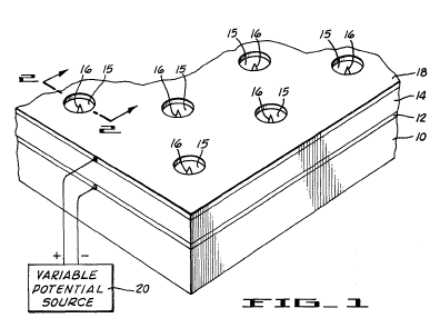
(Via Google Patents))
Spindt's
patented field emitter,[1-2] called a
Spindt cathode, will emit electrons without being heated by a process called
field emission. Not only that, but they would emit under a hundred volts of applied potential in the small dimension structures fabricated by Spindt and his colleagues. One intended application for these electron emitters was for
displays as an updated version of the
cathode ray tube, but there was a fundamental problem.
The problem there was that translating
cathodoluminescence from the high voltages of cathode ray tubes to the low voltages of field emission devices meant that you needed a much higher current to get the same power. High current is just another way of saying a greater number of electrons per second, and all these electrons deposit their
kinetic energy in the
phosphor material. What you get is the same degradation of phosphor screens that was responsible for
burnt-in images in cathode ray tubes, the effect that
screensavers were originally designed to prevent.
A paper in the August 4, 2011, issue of
Electronics Letters by
Jimmy L. Davidson, Emeritus Professor of Electrical Engineering,
Materials Science and Engineering Management, and colleagues at
Vanderbilt University, describes a planar
triode electron device made from
diamond. The diamond layers in the device are made by
reaction of
hydrogen and
methane, a common process for diamond formation.
Diamond is an ideal material for such a device, since it has an extremely low
work function.[4] Because of this low work function, diamond will produce field emission electron beams at low voltage. The device, as shown in the
electron micrograph, is formed by a layer of diamond on a
silicon dioxide insulator. The silicon dioxide substrate is formed on a
silicon wafer. The only unusual requirement in fabrication of such devices is the need to maintain the diamond triodes in a
high vacuum.
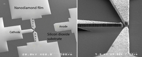
Left, scanning electron microscope image of a nanodiamond transistor. Right, detail of the device, showing the nanodiamond field emitter cantilevered above the insulating silicon dioxide surface. (Images, Davidson Lab, Vanderbilt University). [3]
The diamond triodes can be used at high temperatures, possibly to about 500°C, and they should function at near liquid nitrogen temperatures. It takes
a little trickery to make transistors radiation resistant, but the diamond triodes are inherently
radiation resistant. Said lead author Davidson,
"When I read about the problems at the Fukushima power plant after the Japanese tsunami, I realized that nanodiamond circuits would be perfect for failsafe circuitry in nuclear reactors... It wouldn't be affected by high radiation levels or the high temperatures created by the explosions."[3]
Davidson's diamond triode research was supported by the
U.S. Army.[3]
References:
- C. A. Spindt, "A Thin‐Film Field‐Emission Cathode," Journal of Applied Physics, vol. 39, no. 7 (June 1, 1968), pp. 3504f..
- Charles A. Spindt, Kenneth R. Shoulders and Louis N. Heynick, "Field Emission Cathode Structures And Devices Utilizing Such Structures," US Patent No. 3,755,704, August 28, 1973.
- David Salisbury, "Designing diamond circuits for extreme environments," Vanderbilt University Press Release, Aug. 4, 2011
- L. Diederich, O.M. Küttel, P. Aebi and L. Schlapbach, "Electron affinity and work function of differently oriented and doped diamond surfaces determined by photoelectron spectroscopy," Surface Science, vol. 418, no. 1 (1998), pp. 219-239.
Permanent Link to this article
Linked Keywords: Transistor; electronic circuit; vacuum tube; electronics technician; US Air Force; television set; electrical engineer; General Electric; amateur radio operator; gain; low power; temperature coefficient; temperature sensitive; current; amplifier; transconductance amplifier; Mikoyan-Gurevich MiG-25; Soviet; fighter aircraft; avionics; radar; transmitter; megawatt; AA-6 Acrid air-to-air missile; Wikimedia Commons; field effect transistor; high impedance; gate; control electrode; scientist; thermionic emission; electron; resistance heater; voltage; cathode; anode; Stanford Research Institute; Menlo Park, California; lithography; integrated circuit; Benjamin Franklin; lightning rod; conductor; Maxwell's equations; electromagnetic theory; electric field; field emitter; Spindt cathode; field electron emission; display; cathode ray tube; cathodoluminescence; kinetic energy; phosphor; screen burn-in; screensaver; Electronics Letters; Jimmy L. Davidson; Materials Science; Vanderbilt University; triode; diamond; chemical vapor deposition of diamond; hydrogen; methane; work function; electron micrograph; silicon dioxide; insulator; silicon; wafer; high vacuum; radiation hardening; radiation resistant; silicon on sapphire; U.S. Army; C. A. Spindt; US Patent No. 3,755,704.