A MEMS-FET Memory Cell
March 23, 2011
Before the advent of
stored program computers,
computers were programmed using
plugboards.
Programmers would connect wires from point to point on the computer to complete the necessary
logic circuits for operation. The
ENIAC is one such example. Later computers would have panel switches that would allow input of a simple boot program into
memory. This program was usually a routine that would pass control to a
punched-tape reader that would put a desired program into memory.
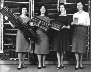
1960s glamor shot.
A photograph showing the evolution of early computer circuitry. Left to Right: Patsy Simmers, holding ENIAC board; Mrs. Gail Taylor, holding EDVAC board; Mrs. Milly Beck, holding ORDVAC board; Mrs. Norma Stec, holding BRLESC-I board.
(U.S. Army Photo No. 163-12-62, Via Wikimedia Commons.
What these techniques had in common is the idea that computer memory involved the connection of wires. In the plugboard case, you could see the actual wire connection; in the switch case, the connection was by a hidden conductor inside the switch. A recent article in
Nature Communications describes a
MEMS memory cell that contains a mechanical switch.[1] Aside from the obvious nostalgia factor, this new memory device can have some advantages over conventional,
non-volatile memory, such as
flash. The MEMS-FET memory element was developed by an international team with members from
Konkuk University (Seoul, Korea), the
Seoul National University (Suwon, Korea) and
Edinburgh University (Edinburgh, UK).
The usual architecture of an
FET memory element is based on the idea that a charged
capacitor connected to the
insulated gate of an FET will affect its
drain-source resistance. Since the gate is insulated, the ideal condition is that the charge will hold forever; well, at least until the
warranty runs out. The situation is complicated somewhat by the fact that we need to either charge or discharge the capacitor in the first place.
Physics comes to the rescue in a
semi-classical form for charging; and a
quantum mechanical form for discharging. Charging is accomplished by "shooting"
electrons through an
insulator in a process called
hot carrier injection. Discharging requires the
quantum tunnelling of electrons from the gate through the insulator.
These processes, which are used in
flash memory, have some disadvantages, the worst of which is the long time needed for the quantum tunnelling to discharge the memory cells. Another
non-volatile memory type,
EEPROM, uses quantum tunnelling for both charging and discharging, and it requires
high voltages to work. The voltages are often generated right on the memory chip; but things happen slowly, at least by computing standards.
Flash memory cells can be charged in about ten microseconds, but they take about ten milliseconds to discharge. Of course, the idea that you've actually found an application for quantum tunnelling erases most objections to this slow speed for
technologists; but the end-users are a little less patient. That's one reason why there's been a lot of research in other non-volatile memory devices, such as
MRAM,
FeRAM,
PRAM and
ReRAM. The MEMS-FET memory cell solves the charging-discharging problem in a very straightforward way, as shown in the figure.
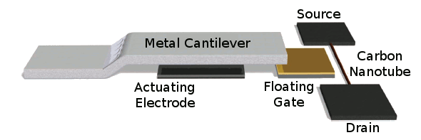
MEMS-FET memory element. The actuation electrode causes the MEMS cantilever to contact the carbon nanotube FET gate, which is built on a storage capacitor. Simplified image from ref. 1. Image licensed by the authors under the Creative Commons Attribution - NonCommercial - Share Alike 3.0 Unported License.
Carbon nanotubes have been proposed for a plethora of non-volatile memory architectures that have a variety of problems. These include slow speed and short data retention time. The mechanical switch approach solves both these problems, and it has the further advantages of extremely
linear operation and
low power operation. The actuator for the MEMS cantilever switch requires just 5 x 10
-14 J.[2] The switching energy loss in a carbon nanotube FET is about the same as for a conventional FET, but the MEMS-FET architecture requires a much shorter switching time. The authors conclude that the power requirements for this memory cell is far less than for flash cell, which is anywhere from 20-1000 nJ.[2]
Flash memory can be reprogrammed anywhere from 10,000 to 100,000 times. MEMS cantilever switches of the type used in this memory device have demonstrated more than 100 million switching cycles. The switching time for the devices were found to be about 130 ns to switch to the "on" state, and 145 ns to switch to the "off" state. Because of the high linearity and high isolation of the switch, it was possible to program
multinary states in the memory cells.[1]
References:
- Sang Wook Lee, Seung Joo Park, Eleanor E. B. Campbell and Yung Woo Park, "A fast and low-power microelectromechanical system-based non-volatile memory device," Nature Communications, vol. 2, no. 3 (March 1, 2011), Article No. 220.
- Supplementary information for ref. 1.
Permanent Link to this article
Linked Keywords: Stored program computer; computer; plugboard; programmer; logic gate; logic circuits; ENIAC; magnetic-core memory; punched-tape; U.S. Army Photo No. 163-12-62; Wikimedia Commons; Nature Communications; microelectromechanical systems; MEMS; non-volatile memory; flash; Konkuk University (Seoul, Korea; Seoul National University (Suwon, Korea); Edinburgh University (Edinburgh, UK); field-effect transistor; FET; capacitor; insulated gate; drain-source resistance; warranty; physics; classical mechanics; quantum mechanics; electrons; electrical insulator; hot carrier injection; quantum tunnelling; flash memory; EEPROM; high voltage; computer engineering; magnetoresistive random access memory; MRAM; ferroelectric RAM; FeRAM; phase-change memory; PRAM; resistive random-access memory; ReRAM; carbon nanotubes; linear operation; low power electronics; Joule; J; N-ary code; multinary.