
Printed Piezoelectrics
October 29, 2018 Microphones are an integral part of many of today's electronic devices. One obvious locale for a microphone is your cellphone, but there are now microphones in consumer electronic devices such as Google Home, the Amazon Echo, and the remote control of Amazon Fire TV that I use to watch far too many science fiction films of the 1950s. I enjoy these films, since these were the films of my childhood. The microphone type in all these devices is the electret microphone, a type that's easily miniaturized and fabricated using planar processing technology. My first microphone, which was an accessory for an inexpensive tape recorder, was a crystal microphone. The active element of this microphone was the piezoelectric material, potassium sodium tartrate tetrahydrate, commonly called Rochelle salt after the place of its first synthesis in about 1675. Just like a crystal wine goblet, the crystal of this microphone was destroyed when the microphone was dropped onto the floor.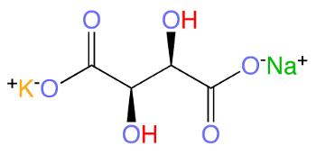
Structural diagram of L-Rochelle salt, potassium sodium tartrate tetrahydrate, KNaC4H4O6.
This inorganic salt typically exists with four waters of hydration.
(Modified Wikimedia Commons image.)
Piezoelectrics are useful for more than just microphones. They also perform the inverse function of turning an oscillating electric field into mechanical movement. In its simplest form, this would be a loudspeaker, but a piezoelectric can be used as an actuator or piezoelectric motor. Unfortunately, the mechanical force is relatively small, primarily because the high impedance of a piezoelectric doesn't allow much of a power transfer at reasonable voltages. Piezoelectrics can also be used as vibration energy harvesters, converting environmental vibration and things such as the force exerted by a gentle breeze to electric power for miniature devices. Piezoelectrics are also used as resonant elements in frequency sources, and quartz, a piezoelectric mineral available as large crystals in nature and later as laboratory grown crystals, has been used in this application since the advent of radio. While thin wafers of quartz were the predominant piezoelectric resonator for a century, surface acoustic wave resonators of other piezoelectric materials such as lithium niobate have become popular now that radio technology has extended to higher frequencies, such as 5.8 gigahertz WiFi.
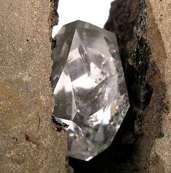
Quartz crystal in a dolomite ore, a "Herkimer diamond" from Herkimer County, New York.
Such quartz crystals were formed in pockets of acidic aqueous solutions of silica in the Carboniferous Period.
This particular crystal growth mechanism, which is used to grow quartz and other crystals in a laboratory, is called hydrothermal synthesis.
(Wikimedia Commons image by Robert Lavinsky.)
Materials scientists are always searching for materials having better properties than existing materials. One property that's important for a piezoelectric material is its electromechanical coupling coefficient, the quantity that relates how well the material can convert electrical energy into mechanical energy, and it varies widely between materials and their crystallographic directions. There are piezoelectrics other than quartz that are used in their crystalline form, many with properties that are superior to quartz. Among these are lithium tantalate (LiTaO3), lithium niobate (LiNbO3), barium titanate (BaTiO3), lithium tetraborate (Li2B4O7), aluminum phosphate (aluminum phosphate (AlPO4, Berlinite), gallium phosphate (GaPO4), lead magnesium niobate (PMN), and lead zirconate titanate (PZT). While slices of single crystals offer the best piezoelectric conversion of electrical power to mechanical motion, and vice-versa, textured ceramic layers of piezoelectric materials will give a response. They're only about a tenth as efficient, but that's often enough in some applications. Films of PZT, Zinc oxide (ZnO) or aluminum nitride (AlN) are sometimes layered onto semiconductor wafers to give an added piezoelectric functionality. In particular, AlN is used to fabricate thin-film bulk acoustic resonators for microwave filters.
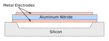
As easy as this - An aluminum nitride (AlN) thin-film bulk acoustic resonator (FBAR) on silicon.
The speed of longitudinal acoustic wave in AlN is about 10,000 meters/second, so a resonant half wavelength in a one micrometer layer corresponds to a frequency of about 20 GHz.
(Created using Inkscape.)
The usual deposition process for piezoelectric thin films is physical vapor deposition, a vacuum deposition process that has a large enough deposition rate to prepare micrometer thickness layers, as in the FBAR example in the above figure. A method of printing piezoelectrics would allow an easier production of large area and thicker layers. That was the object of research on the piezoelectric, gallium phosphate (GaPO4) by a team of Australian and German scientists from the Royal Melbourne Institute of Technology (RMIT, Melbourne, Australia), the University of New South Wales (New South Wales, Australia), and the University of Münster (Münster, Germany). This research is reported in an open access paper in Nature Communications.[1-2]
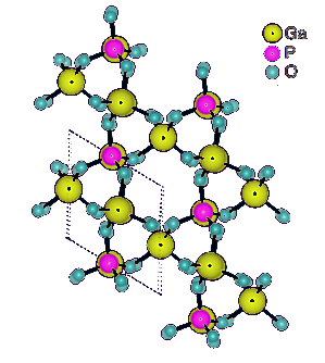
Structure of gallium phosphate (GaPO4) at unit cell thickness.
Gallium phosphate (α)-GaPO4), is a piezoelectric material that is iso-structural with α-quartz.
It has trigonal symmetry with cell parameters of a = 0.487 nm and c = 1.105 nm and trigonal angle γ = 120°.[1]
(Australian Research Council Centre of Excellence in Future Low-Energy Electronics Technologies image, modified.)
The process, as shown in the figure, is quite simple. A substrate is first wetted with a thin layer of gallium oxide (Ga2O3) by contact with the normally oxidized surface of liquid gallium. Van der Waals forces cause the exfoliation and adsorption of the gallium oxide layer.[2] This step is easy, since the melting point of gallium is just 29.77 °C. This film of gallium oxide is then exposed to flowing vapors of phosphoric acid at 350 °C, a very low temperature for wafer processing.[1-2]
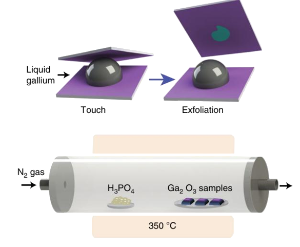
Process for creation of gallium phosphate layers. Van der Waals forces allow transfer of the gallium oxide layer from a liquid droplet of gallium to a substrate. A chemical vapor reaction transforms the gallium oxide to gallium phosphate nanosheets.(Australian Research Council Centre of Excellence in Future Low-Energy Electronics Technologies image.)
Unit cell nanosheets showed a large out-of-plane piezoelectric coefficient of 7.5 ± 0.8 picometers/volt.[1-2] Bulk gallium phosphate has a significantly higher thermal stability and a higher piezoelectric coefficient than quartz, so the same might be expected for these nanosheets.[1] The α-phase of bulk gallium phosphate is stable up to 930 °C.[1] This synthesis technique produces gallium phosphate nanosheets of unit cell thickness that could potentially reach centimeter dimension.[1] This printing process is also suitable for creation of free-standing gallium phosphate nanosheets.[1] computational support for this study was provided by the Pawsey Supercomputer Centre, named after the Australian radio astronomer, Joseph Lade Pawsey (1908-1962).[2]
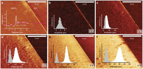
Atomic force microscope imaging of the gallium phosphate nanosheets, including piezoelectric measurements at various applied voltages. (Australian Research Council Centre of Excellence in Future Low-Energy Electronics Technologies image.)
References:
- Nitu Syed, Ali Zavabeti, Jian Zhen Ou, Md Mohiuddin, Naresh Pillai, Benjamin J. Carey, Bao Yue Zhang, Robi S. Datta, Azmira Jannat, Farjana Haque, Kibret A. Messalea, Chenglong Xu, Salvy P. Russo, Chris F. McConville, Torben Daeneke. and Kourosh Kalantar-Zadeh, "Printing two-dimensional gallium phosphate out of liquid metal," Nature Communications, v. 9, Article no. 3618 (2018), DOI 10.1038/s41467-018-06124-1. This is an open access paper with a PDF file here.
- Pushing 'print' on large-scale piezoelectric materials, Australian Research Council Centre of Excellence in Future Low-Energy Electronics Technologies Press Release, September 6, 2018.