Exfoliated Graphite
November 26, 2018 Lead, which was used in many consumer applications, including as a gasoline additive, has been banned since the middle of the 20th century because of its toxicity. That's why many people are confused about the existence of lead pencils. Lead pencils are actually made from graphite, not lead. As explained in a informative blog article,[1] the graphite material of the first pencils was initially thought to be a form of lead, and it was called plumbago after the Latin word for lead (plumbum, from which we get the chemical symbol for lead, Pb). Plumbago was discovered several centuries ago as an ore deposit in Cumbria, England. It was extensively used as a mold-release agent in the casting of cannon balls. While modern analytical techniques were not available at that time, it should have been easy to distinguish graphite from lead by its density. Graphite has a density of about 2.2 g/cc, while lead has a density of 11.34 g/cc. A large density difference would have been expected even if plumbago wasn't lead, but another compound of lead, such as lead carbonate, since lead carbonate's density is about 6.6 g/cc. Eventually, it was found that the material was not lead, but the term is still associated with pencils.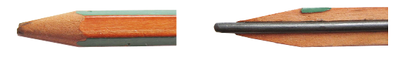
Detail of lead pencil construction. Modern pencil leads are formed as a composite of clay and graphite powder and are encased in wood. (Wikimedia Commons image, modified.)
Graphite makes an excellent pencil material, since flakes of carbon are easily rubbed from graphite because of its layered structure. Graphite is composed of sheets of graphene loosely held atop each other by weak van der Waals forces. The difference in bond strength between layers can be seen by the difference in the carbon-carbon atomic distance, 0.142 nm in the graphene plane, and 0.335 nm between planes.
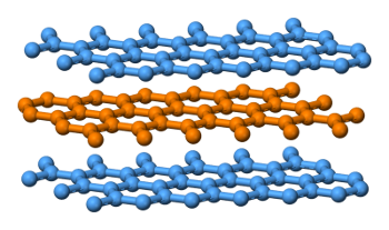
Layered structure of graphite.
Carbon atoms in the planes are tightly bonded, while the planes are bonded together by weak van der Waals forces.
(Wikimedia Commons image by Benjah-bmm27.)
The spacing between graphene layers is larger than the size of many small molecules. water, for example, has a size of about 0.275 nanometers. For this reason, graphite can be intercalated; that is, molecules and ions can be inserted between the layers. Intercalation will slightly expand the gap between the graphene sheets. Metal halides, such as ferric chloride, FeCl3, are common compounds for graphite intercalation. While intercalation does modify the physical properties of graphite, taking intercalation to an extreme by causing a large layer separation leads to exfoliation, a breakup of graphite into its individual layers. The term, exfoliation, comes from the word, folio, which is an individual sheet of paper. Exfoliation of graphite can be achieved by heating ferric chloride intercalated graphite at several hundred degrees Celsius. One early application of exfoliated graphite was as a high temperature gasket material (Grafoil®).[3] Since layers of graphite are the important electronic material, graphene, there has been much research in exfoliation of graphite.[4-6] Exfoliation of graphite and layered compounds results in materials with surface areas greater than 1000 square meters per gram. Such materials will have enhanced surface activity, and they are useful as electrodes in batteries and supercapacitors. When used as part of a composite, exfoliated materials act as molecularly thin barriers and electromagnetic shields by virtue of their conductivity.[4] Only a small quantity of exfoliated graphene platelets, of the order of 2-5 weight percent, is required to make a shielding composite.
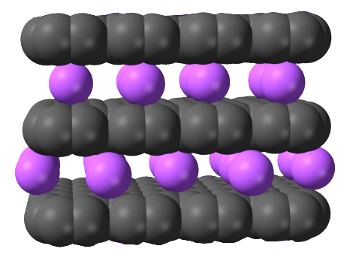
Graphite can be electrochemically loaded with potassium ions using an aqueous Potassium hydroxide (KOH) electrolyte and then exfoliated.[7]
In this illustration of graphite intercalated with potassium ions, the carbon atoms are naturally represented as black.
(Modified Wikimedia Commons image by Ben Mills.)
While graphene is seen as a breakthrough electronic material, it has a size problem. Silicon wafers are as large as twelve inches, and such sizes are needed to make production of integrated circuits economical, but graphene has only been produced in small flakes. That's why research is being done on graphite exfoliation as one technique for production of large area graphene sheets. Exfoliation of graphene and similar materials is the topic of a recent publication by researchers from the Massachusetts Institute of Technology (Cambridge, Massachusetts), MIT Lincoln Laboratory (Lexington, Massachusetts), Yonsei University (Seoul, Republic of Korea), Ohio State University (Columbus, Ohio), the Georgia Institute of Technology (Atlanta, Georgia), the University of Texas at Dallas (Richardson, Texas), the University of Virginia (Charlottesville, Virginia), and the University of Notre Dame (Notre Dame, Indiana).[8-9] Their exfoliation technique is different from chemical techniques. The traditional way of removing graphene sheets from graphite is the one discovered by Andre Geim and Konstantin Novoselov, who were awarded the 2010 Nobel Prize in Physics for their pioneering work on graphene.[10] They used cellophane tape to peel off single layers of graphene carbon from bulk graphite. As is easily realized, this method does not scale well to the production of large area graphene substrates for electronic devices.[8-9] It's also difficult to produce graphene layers on other materials since nucleation is difficult.[8] This new exfoliation process allows for the rapid wafer-scale (5 centimeter diameter) production of not only monolayers of carbon, but also monolayers of hexagonal boron nitride (h-BN), tungsten disulfide (WS2), tungsten diselenide (WSe2), molybdenum disulfide (MoS2), and molybdenum diselenide (MoSe2).[8-9] First, a thick stack of monolayers one of one of these materials is grown on top of a sapphire wafer, then a 600-nanometer-thick nickel film is deposited onto the top of the stack.[9] Since the materials adhere more strongly to the nickel than sapphire, lifting the nickel film removes the material stack.[9] When a second nickel film is deposited on the bottom of the stack, it's possible to peel off single-atom thick monolayers of those materials.[9] After this first monolayer is removed, the process can be repeated until the stack is depleted (see figure).[9]
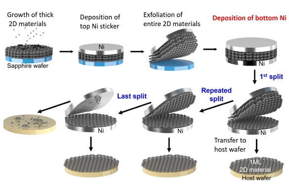
Graphene exfoliation process by which wafer-scale graphene is produced. (MIT image.)
The research team plans to demonstrate several electronic devices based on the monolayers produced by this process, including flexible devices and a nonvolatile memory array.[9] They've already fabricated working arrays of field-effect transistors having just few atoms thickness.[9]
References:
- Stephanie Huesler, "Plumbago vs. Graphite," History Undusted, May 31, 2013.
- Minzhen Cai, Daniel Thorpe, Douglas H. Adamson and Hannes C. Schniepp, "Methods of graphite exfoliation," Journal of Materials Chemistry, vol. 22, no. 48 (September 12, 2012), pp. 24992-25002, DOI: 10.1039/C2JM34517J.
- James H Shane, Robert J Russell, and Raymond A Bochman, "Flexible graphite material of expanded particles compressed together," U.S. Patent No. 3,404,061, March 21, 1962.
- Valeria Nicolosi, Manish Chhowalla, Mercouri G. Kanatzidis, Michael S. Strano, and Jonathan N. Coleman, "Liquid Exfoliation of Layered Materials," Science, Vol. 340, no. 6139 (June 21, 2013), Article no. 1226419, DOI: 10.1126/science.1226419.
- D. D. L. Chung, "A review of exfoliated graphite," Journal of Materials Science, vol. 51, no. 1 (January, 2016), pp 554-568, https://doi.org/10.1007/s10853-015-9284-6.
- Richard E.Stevens, Sydney Ross, and Sheldon P.Wesson, "Exfoliated graphite from the intercalate with ferric chloride," Carbon, vol. 11, no. 5 (October, 1973), pp. 525-530, https://doi.org/10.1016/0008-6223(73)90312-6.
- Prashant Tripathi, Ch. Ravi Prakash Patel, M. A. Shaz, and O. N. Srivastava, "Synthesis of High-Quality Graphene through Electrochemical Exfoliation of Graphite in Alkaline Electrolyte," arXiv, October 28, 2013.
- Jaewoo Shim, Sang-Hoon Bae, Wei Kong, Doyoon Lee, Kuan Qiao, Daniel Nezich, Yong Ju Park, Ruike Zhao, Suresh Sundaram, Xin Li, Hanwool Yeon, Chanyeol Choi, Hyun Kum, Ruoyu Yue, Guanyu Zhou, Yunbo Ou, Kyusang Lee, Jagadeesh Moodera, Xuanhe Zhao, Jong-Hyun Ahn, Christopher Hinkle, Abdallah Ougazzaden, and Jeehwan Kim, "Controlled crack propagation for atomic precision handling of wafer-scale two-dimensional materials," Science (Early Release, October 11, 2018), Article no. eaat8126, DOI: 10.1126/science.aat8126.
- Helen Knight, "Researchers quickly harvest 2-D materials, bringing them closer to commercialization," MIT Press Release, October 11, 2018.
- K. S. Novoselov, A. K. Geim, S. V. Morozov, D. Jiang, Y. Zhang, S. V. Dubonos, I. V. Grigorieva and A. A. Firsov, "Electric Field Effect in Atomically Thin Carbon Films," Science, vol. 306, no. 5696 (October 22, 2004), pp. 666-669.