Si2BN - A Graphene Analog
March 17, 2016
The
metals available to ancient man were the
metallic elements found in their free form in
nature, or those extracted by
heating of some common ores. Since gold is the least reactive metal, it occurs in nature as the metal, itself, so it was the first metal used by man. Our
ancestors soon discovered how smelting of ores can release silver, mercury, copper, lead, tin, and iron.
All of these metals are relatively soft, and the major reason that iron was useful was because the accidental incorporation of
carbon transformed it into
steel. Eventually, it was discovered that mixing some metals in a proper proportion gave
alloys with superior
mechanical properties. One example of this is
bronze, an alloy of copper and tin.
Bronze is stronger than copper, and it had sufficient properties to launch a new age of man called the
Bronze Age. While copper has a
tensile strength of 32
ksi, adding a little tin boosts this to about 45 ksi, while addition of just 1%
phosphorus to produce
phosphor bronze results in an alloy with a tensile strength of about 120 ksi.
As
metallurgy achieved a
scientific basis, it was discovered that exceptional alloys could be made when several elements were combined; and, why just stop at a few, when a little pinch of one or another element has a beneficial effect. Some modern alloys are made from ten or more elements, each of which having its own particular purpose. One example is MAR-M-247,[2] a
Martin Marietta nickel-based
superalloy used for the hottest parts of
turbine engines, such as
turbine blades. This alloy, which resists
oxidation and
corrosion and has excellent strength at
high temperature, has the following composition (
mass-%):
Additionally, a little
hafnium or
zirconium can be added to enhance
ductility.
Research on
graphene, the
atomic layer thick
allotropic form of carbon, accelerated after 2004 when a technique was discovered to cleave graphene layers from
graphite and attach them to
crystal wafers for measurement. This discovery was significant enough for the originators of this process,
Andre Geim and
Konstantin Novoselov, to earn the 2010
Nobel Prize in Physics.
Taking a
cue from alloy metallurgy,
scientists decided that if one type of atom works well as a
two-dimensional material, perhaps similar atomic layers incorporating more than one element would have some unique properties. That's why we now have
experiments involving
molybdenum disulfide (MoS
2),
molybdenum diselenide (MoSe
2), and
tungsten diselenide (WSe
2). I wrote about some properties of these atomic layer materials in some previous articles (
Molybdenum Disulfide Circuitry, December 9, 2011,
Quilting Semiconductors, September 26, 2014, and
Light-Emitting Diodes of Tungsten Diselenide, March 17, 2014).
These two-dimensional materials are somewhat of a
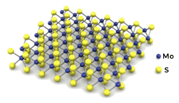
cheat. Unlike graphene, it takes three layers to get one
compound layer. A group of scientists from the
Institute of Electronic Structure and Laser (IESL, Heraklio, Crete, Greece),
Daimler AG (Ulm, Germany), and the
University of Kentucky (Lexington, Kentucky) decided that it would be interesting to see what single layer compounds of multiple types of atoms would be
theoretically possible. They've found a candidate in
Si2BN.[3-5]
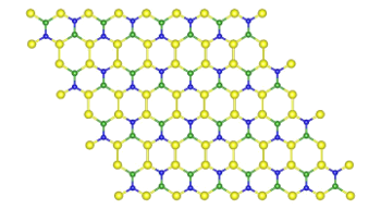
This material is a modification of the
hexagonal crystal form of
boron nitride, (α-BN), which is layered like graphite (see figure). Both the
boron and
nitrogen atoms of boron nitride are in the
plane of the single sheet. However, the material is an
insulator, and it's not as useful as graphene.
At this point, the Si
2BN material has just been predicted theoretically, it hasn't been made. The research team used an
ab initio calculation of the single-atomic-layer Si
2BN structure in which all of the atoms connect by with
sp2 bonding; and, like graphene, there's no out-of-plane
buckling.[3]
This new material has the advantage over the previously mentioned selenides and sulfides that it forms in a true single atomic layer. Also, its elements are abundant and quite inexpensive.[4] They're from the first two rows of the
periodic table, and low
atomic number elements are more common than those higher in the periodic table. The new material is much more stable than the graphene alternatives, and it was the only way that these three elements could bond as a single layer.[4]
Although the material has the same hexagonal structure as graphene, the atomic bonds are of different
lengths.[4] While graphene has excellent
mechanical properties, it isn't a
semiconductor, and this precludes its easy application in
electronic circuitry. The Si
2BN material is metallic, but it can be easily made to be semiconducting by attaching other elements to the silicon atoms.[4] Also, the presence of silicon makes it a candidate material for
hydrogen storage.[3]
The Si
2BN material should be quite stable. Says
Madhu Menon,
physicist and
coauthor of the
paper describing this
research,
"We used simulations to see if the bonds would break or disintegrate - it didn't happen... We heated the material up to 1,000-degree Celsius and it still didn't break."[4]
As they say, "
The proof of the pudding is in the eating," and Menon is eager to have someone
synthesize this material.
"We are very anxious for this to be made in the lab... The ultimate test of any theory is experimental verification, so the sooner the better!... We know that silicon-based technology is reaching its limit because we are putting more and more components together and making electronic processors more and more compact, but we know that this cannot go on indefinitely; we need smarter materials... This discovery opens a new chapter in material science by offering new opportunities for researchers to explore functional flexibility and new properties for new applications... We can expect some surprises."[4]
References:
- Hugh G. Evelyn-White, Trans., "Hesiod, The Homeric Hymns and Homerica," William Heinemann/The Macmillan Co. (London/New York, 1914), pp. 12-13.
- W. Danesi, J. Hockin, and C. Lund, "Tungsten containing alloy," US Patent No. 3,759,707, September 18, 1973.
- Antonis N. Andriotis, Ernst Richter, and Madhu Menon, "Prediction of a new graphenelike Si2BN solid," Phys. Rev. B, vol. 93, no. 8 (February 15, 2016), Document no. 081413, DOI:http://dx.doi.org/10.1103/PhysRevB.93.081413.
- UK Physicist Discovers New 2D Material that could Upstage Graphene, University of Kentucky Press Release, February 29, 2016.
- Dr. Madhu Menon Proposes New 2D Material, YouTube Video by the University of Kentucky, February 26, 2016. Note that the chemical symbol for boron in the periodic table of this video is wrong.


