Graphene from Nickel
June 11, 2014
Most
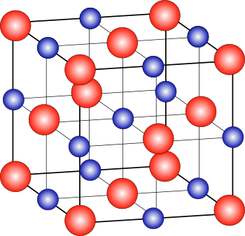
materials solidify into
crystals, which are
regular arrays of atoms. That's a simple consequence of
thermodynamics, since such a regular arrangement of atoms is a low
entropy state; and, at least for
ions such as those of
sodium and
chlorine, such an arrangement leads to a higher
bonding energy between
atoms.
Essentially, you're minimizing the
Gibbs free energy G, which is a
function of both
reaction enthalpy (the bonding energy)
H and the entropy
S at a given
absolute temperature T; viz.,
G = H - TS.
In a perfect world, atoms would always arrange themselves in neat arrays, but in the real world, everything has
defects, and
atoms move around. Atoms will remain in placed at
absolute zero, essentially because atomic movement is
how temperature is defined. Atoms remain in place until about 80% of a material's
melting point in absolute temperature units (
kelvin). Above that, atom motion is used to beneficial effect in
annealing, which removes internal
strain.
The
industrial revolution was built not only by
steam, but also by
steel.
Iron is a plentiful and inexpensive material, and the 1855
Bessemer process, which had actually been practiced for quite a time before
Henry Bessemer's patent, allowed production of very pure iron in large quantity. Pure iron is soft and
ductile, but a pinch of
carbon transforms iron to
higher strength steel.
Carbon is a small atom (77
picometers (pm) when
bonded as sp3) compared with iron (126 pm), so carbon atoms are relatively mobile in iron. Since steel is such an important material, the
diffusion (movement) of carbon atoms in iron has been thoroughly researched. Carbon diffusion in iron follows an
Arrhenius-type law,
where
D is the
diffusion coefficient (measured in
cm2/
sec), the
activation energy is 0.873
electron volts,
kB is the
Boltzmann constant and
T is the
absolute temperature. Because of this is an
exponential function, the diffusion coefficient varies by many
orders of magnitude between
room temperature and the melting point of iron, 1538 °C.
Nickel, like iron, is in the first
transition metal series of the
Periodic Table, and it's separated from iron by just one
chemical element,
cobalt. The crystal structure of nickel (
face-centered cubic) has its atoms more closely spaced than the
body-centered cubic structure of iron, so the diffusion of carbon in nickel is much smaller.
At high temperatures, the diffusivity of carbon in nickel is more than a million times smaller than that for iron.[1] However, if your goal is to transport carbon through a very thin layer of nickel, the diffusivity is more than enough. The
solubility of carbon in nickel is also a hundred times less than that of carbon in iron.[1]
Scientists from the
Department of Mechanical Engineering, the
University of Michigan (Ann Arbor, Michigan), the
Department of Mechanical Engineering, the
Massachusetts Institute of Technology (Cambridge, Massachusetts), and
Guardian Industries Corporation (Carleton, Michigan) have used these properties of carbon in nickel to devise a process for production of large
area graphene sheets on
silica.[2-3]
The first process for creation of graphene was the use of
Scotch tape to exfoliate atomically thin graphene sheets from
graphite. It was a crude process, but it was good enough to win the 2010
Nobel Prize in Physics for its discoverers,
Andre Geim and
Konstantin Novoselov. It would be difficult to
commercialize graphene
devices using this technique.
Another process for production of graphene is to grow it on a
metal, such as nickel or
copper, but it's only useful when removed from the metal. Although the growth of large areas of graphene has become common, removal of the graphene from its growth
substrate is a major issue.[3] That's the problem tackled in this latest study.
The
research team, led by
A. John Hart of MIT, developed a process for production of graphene on silica glass (SiO
2) by using
chemical vapor deposition (CVD) to grow graphene from
ethylene on both sides of a nickel film
deposited on the glass substrate. A subsequent dry
mechanical delamination using
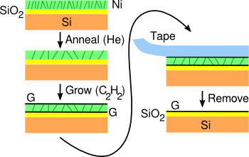
adhesive tape removes the nickel layer and the top graphene layer to leave a layer of graphene on glass (see figure).[2]
 | The graphene-on-glass process.
Graphene can be grown on both sides of a nickel film on a glass substrate.
(Original image by the study authors, redrawn for clarity, via MIT) |
The graphene is produced in
micrometer-sized,
monolayer to multiple-layer domains. There's greater than 90% coverage across a
centimeter dimension substrate, which was the size limit for their CVD system.[2] An important part of the removal process is a strain-relief anneal of the nickel film prior to graphene deposition. Although the nickel film remains adherent to the glass even after formation of the graphene, it can be mechanically removed after deposition.[2]
Says MIT's Hart,
"We still need to improve the uniformity and the quality of the graphene to make it useful... The ability to produce graphene directly on nonmetal substrates could be used for large-format displays and touch screens, and for 'smart' windows that have integrated devices like heaters and sensors."[3]
The work was supported by the
National Science Foundation, the
Air Force Office of Scientific Research, and Guardian Industries.[3]
References:
- J. J. Lander, H. E. Kern and A. L. Beach, "Solubility and Diffusion Coefficient of Carbon in Nickel: Reaction Rates of Nickel‐Carbon Alloys with Barium Oxide," J. Appl. Phys., vol. 23, no. 12 (December 1, 1052), p.1305ff., DOI:10.1063/1.1702064.
- Daniel Q. McNerny, B. Viswanath, Davor Copic, Fabrice R. Laye, Christophor Prohoda, Anna C. Brieland-Shoultz, Erik S. Polsen, Nicholas T. Dee, Vijayen S. Veerasamy and A. John Hart, "Direct fabrication of graphene on SiO2 enabled by thin film stress engineering," Scientific Reports, vol. 4 (May 23, 2014), Article no. 5049 (doi:10.1038/srep05049). This is an open access article with a PDF file available, here.
- David L. Chandler, "A new way to make sheets of graphene," MIT Press Release, May 23, 2014.


