Optical Yagi-Uda Nanoantennas
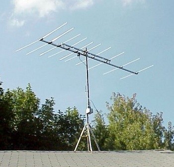
April 25, 2012 Light is an electromagnetic wave, just like radio, so it should be possible to scale radio antenna designs to function for light. The critical dimensions in antennas need to be about the same as the wavelength of the electromagnetic radiation. That's why AM radio towers, which transmit frequencies of about a megahertz, are more than a hundred meters high; and the Wi-Fi antenna on your wireless router (2.45 GHz) is just a few inches long. Since visible light has a wavelength of about 500 nanometers, optical antennas have only become possible with the advent of routine fabrication of nanoscale structures. I wrote about optical antennas in the context of solar energy conversion in a previous article (Optical Antennas, June 13, 2011). The Yagi-Uda antenna has been a popular antenna type for more than eighty years. Its main advantage is that it's directional and offers gain over the isotropic; that is, it concentrates its electromagnetic energy in one direction for a transmitter. For a receiver, it enhances sensitivity in one direction, while at the same time rejecting noise away from that direction. This antenna concept was published in Japanese by Shintaro Uda and Hidetsugu Yagi, but it was called a Yagi antenna in the West, since Yagi published descriptions in English. | This Yagi-Uda antenna sits atop the roof of my house. It was part of a my daughter's 1998 science fair project. The antenna is a Winegard HD6065P High Definition FM Antenna. (FM Radio Detection of Meteors Web Site). |
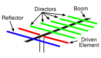
 | Schematic diagram of a Yagi-Uda antenna. (Illustration by author, rendered using Inkscape). |
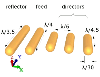
 | An optical Yagi-Uda antenna based on gold nanorods. At a wavelength of 1550 nm, the area occupied by the nanoantenna is about 400 x 400 nm. (Fig. 2 of ref. 2, via the arXiv Preprint Server)[2]. |
 |
| Two optical Yagi-Uda antennas can be used as a mean of transmitting optical signals across a chip, or between chips, without use of an optical waveguide. (Fig. 11 of ref. 2, via the arXiv Preprint Server).[2] |
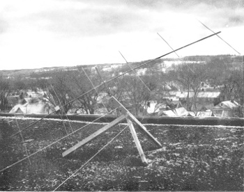
 | My senior high school science fair project included this Yagi-Uda antenna I built from copper piping for a radio telescope. This photograph shows its placement on the school roof (43.100903° latitude, -75.232664° longitude). (click for larger image). |
References:
- Hidetsugu Yagi, "Variable Directional Electric Wave Generating Device," US Patent No. 1,860,123, May 24, 1932.
- Ivan S. Maksymov, Isabelle Staude, Andrey E. Miroshnichenko and Yuri S. Kivshar, "Optical Yagi-Uda nanoantennas," arXiv Preprint Server, April 2, 2012.
- J.D. Kraus, "Antennas," McGraw-Hill (New York, 1988).
- Ivan S. Maksymov, Isabelle Staude, Andrey E. Miroshnichenko and Yuri S. Kivshar, "Optical Yagi-Uda nanoantennas," arXiv Preprint Server, April 2, 2012.