Ohm's Law at the Atomic Scale
January 13, 2012 Electrical current is the flow of electrons. This is expressed in the practical definition of current as amperes. An ampere is the movement of a coulomb of electrons past a measurement point in one second. A coulomb is 6.241 x 10¹⁸ electrons, which is a lot of electrons. I wrote "practical definition," since this isn't the formal definition of an ampere proffered by the International Bureau of Weights and Measures; viz.,The ampere is that constant current which, if maintained in two straight parallel conductors of infinite length, of negligible circular cross-section, and placed 1 metre apart in vacuum, would produce between these conductors a force equal to 2 x 10⁻⁷ newton per metre of length.[1]You can see why the practical definition is more popular. Since current is a flow, educators have developed an hydraulic analogy for electricity in which an electrical current's companion, voltage, is a pressure differential. A constriction in a pipe leads to a resistance to flow, in analogy to electrical resistance. In electrical circuits, the resistance is related to the voltage and current by Ohm's law,
R = V/Iin which R is the resistance in ohms, V is the voltage in volts, and I is the current in amperes. The resistance of a wire depends on the material that it's made from, its length, and its cross-sectional area,
R = ρ x length / areain which ρ is the resistivity, a material property. As expected, long wires, and thin wires, have high resistance. Wires, and conductive traces on integrated circuits, are the pipes that carry electrons. However, electrons are quantum mechanical objects, and they might behave differently when confined to small channels. Ohm's law might break down. Scientists have now tested the scaling of Ohm's law to a conductor just four atoms wide and one atom tall, and it seems to still hold true.[2-6] The research, done by a multinational team from the University of New South Wales, Purdue University, the University of Melbourne, and the IBM Zurich Research Laboratory, was published in the January sixth issue of Science.[2] The paper's lead author is Bent Weber, a Ph.D. candidate at the Australian Centre of Excellence for Quantum Computation and Communication Technology at the University of New South Wales. Michelle Simmons, Director of the Centre and a coauthor, was named New South Wales Scientist of the Year for 2011 by the Australian government.[7]
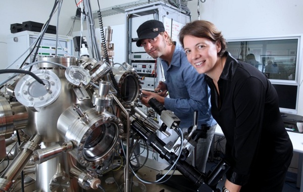
 Bent Weber and Michelle Simmons of the University of New South Wales. An ultra high vacuum (UHV) system, as shown in this photograph, is required to undertake research on atomically clean surfaces. (Photograph courtesy of Michelle Simmons. Used with permission.)
The research team used a scanning tunneling microscope (STM) to fabricate conductive wires that were twenty times smaller than the copper conductors in microprocessors.[4] A silicon surface was first covered with hydrogen. An STM tip desorbs the hydrogen in the shape of the wire, and the surface was then doped with phosphorus atoms, an n-type dopant that increases conductivity in the patterned wire.
The dopant density was high, with phosphorus atoms sitting less than a nanometer from each other. These doped traces were encased with other silicon atoms to protect them. [2]
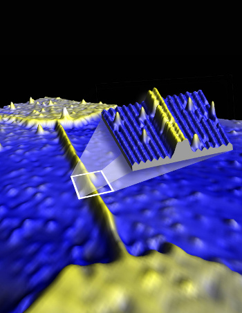
 | STM image of a wire patterned on a silicon wafer. The scan lines and individual atoms can be seen in the inset image. (Image courtesy of Bent Weber, the Univeristy of New South Wales. Used with permission.) |
"Over the past 50 years this paradigm has established the microelectronics industry as one of the key drivers for global economic growth... We are on the threshold of making transistors out of individual atoms... But to build a practical quantum computer we have recognized that the interconnecting wiring and circuitry also needs to shrink to the atomic scale."[4,5]A video summary of these experiments can be found here.[8]
References:
- Unit of electric current (ampere), SI brochure, Section 2.1.1.4, Bureau International des Poids et Mesures.
- B. Weber, S. Mahapatra, H. Ryu, S. Lee, A. Fuhrer, T. C. G. Reusch, D. L. Thompson, W. C. T. Lee, G. Klimeck, L. C. L. Hollenberg and M. Y. Simmons, "Ohm's Law Survives to the Atomic Scale," Science, vol. 335, no. 6064 (January 6, 2012), pp. 64-67.
- David K. Ferry, "Perspective-Applied Physics, Ohm's Law in a Quantum World," Science, vol. 335, no. 6064 (January 6, 2012), pp. 45-46.
- Mary O'Malley, "Wires shrink to atomic scale," Univeristy of New South Wales Press Release, January 6, 2012.
- Greg Kline, "Down to the wire for silicon: Researchers create a wire 4 atoms wide, 1 atom tall," Purdue University Press Release, January 5, 2012.
- John Matson, "Ohm Run: One-Atom-Tall Wires Could Extend Life of Moore's Law," Scientific American, January 5, 2012.
- Deborah Smith, "Scientist of year looks at big picture by thinking small," Sydney Morning Herald, November 24, 2011.
- Univeristy of New South Wales video about this discovery is available, here.
- B. Weber, S. Mahapatra, H. Ryu, S. Lee, A. Fuhrer, T. C. G. Reusch, D. L. Thompson, W. C. T. Lee, G. Klimeck, L. C. L. Hollenberg and M. Y. Simmons, "Ohm's Law Survives to the Atomic Scale," Science, vol. 335, no. 6064 (January 6, 2012), pp. 64-67.