Vacuum Tube Redux
August 9, 2011 The transistor and I were born at about the same time, at the end of 1947. Useful and inexpensive transistors weren't available until many years thereafter, so it's no surprise that the first electronic circuits I built used vacuum tubes. I was aided in my electronics education by two neighbors, one of whom was a civilian electronics technician for the US Air Force. He repaired television sets in his home as a side job, and he gave me many old television sets that I harvested for tubes and components. The other neighbor was an electrical engineer who worked at a military electronics division of General Electric. He was also an amateur radio operator, and "hams," as they are called, are always good at proselytizing their craft. Living in between these two, I got useful hardware from the North side of my house, and useful knowledge from the South side. It took some time for transistors to displace vacuum tubes, especially in certain applications. Early transistors had very low gain, and they were suitable just for low power applications. They were temperature sensitive to the point that they wouldn't work at all at what would be considered modest temperatures today. The first transistors were also current amplifiers, not transconductance amplifiers like vacuum tubes, which led to other application problems. It was therefore no surprise, at least to those engineers who worked with both vacuum tubes and transistors, that the Mikoyan-Gurevich MiG-25, a very successful Soviet fighter aircraft that saw first active duty in 1970, was found to have most of its avionics implemented with vacuum tubes. It's powerful radar system had a transmitter capable of sending radar pulses of about half a megawatt! The MIG-25 was produced through 1984. | A Soviet MiG-25 interceptor aircraft armed with four AA-6 Acrid air-to-air missiles. (Via Wikimedia Commons). |
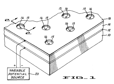
 | (Via Google Patents). |
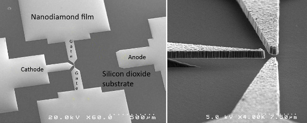
 Left, scanning electron microscope image of a nanodiamond transistor. Right, detail of the device, showing the nanodiamond field emitter cantilevered above the insulating silicon dioxide surface. (Images, Davidson Lab, Vanderbilt University). [3]
The diamond triodes can be used at high temperatures, possibly to about 500°C, and they should function at near liquid nitrogen temperatures. It takes a little trickery to make transistors radiation resistant, but the diamond triodes are inherently radiation resistant. Said lead author Davidson,
"When I read about the problems at the Fukushima power plant after the Japanese tsunami, I realized that nanodiamond circuits would be perfect for failsafe circuitry in nuclear reactors... It wouldn't be affected by high radiation levels or the high temperatures created by the explosions."[3]Davidson's diamond triode research was supported by the U.S. Army.[3]
References:
- C. A. Spindt, "A Thin‐Film Field‐Emission Cathode," Journal of Applied Physics, vol. 39, no. 7 (June 1, 1968), pp. 3504f..
- Charles A. Spindt, Kenneth R. Shoulders and Louis N. Heynick, "Field Emission Cathode Structures And Devices Utilizing Such Structures," US Patent No. 3,755,704, August 28, 1973.
- David Salisbury, "Designing diamond circuits for extreme environments," Vanderbilt University Press Release, Aug. 4, 2011
- L. Diederich, O.M. Küttel, P. Aebi and L. Schlapbach, "Electron affinity and work function of differently oriented and doped diamond surfaces determined by photoelectron spectroscopy," Surface Science, vol. 418, no. 1 (1998), pp. 219-239.
- Charles A. Spindt, Kenneth R. Shoulders and Louis N. Heynick, "Field Emission Cathode Structures And Devices Utilizing Such Structures," US Patent No. 3,755,704, August 28, 1973.