Tikalon Header

Molybdenum Disulfide Circuitry

December 9, 2011

I was introduced to molybdenum disulfide (molybdenite, MoS2) very early in my scientific career. As part of my dissertation project, I had to repeatedly remove and replace a very large flange in a vacuum system that operated at high temperature. The only gasket material that would work at these tempertures was copper, and the gasket needed to be compressed between knife-edges in the flange and seat by tightening a multitude of stainless steel bolts.

This was a tedious process that involved a
torque wrench, or just my calibrated wrists when I couldn't find the wrench; but the tightening task was made easier by using molybdenum disulfide as a thread lubricant. Lubrication is the most common use of molybdenum disulfide.

MoS2 is effective in this application because it's a layered material much like
graphite with easy slip planes. Now that graphite, in the form of graphene, is being used for electronic circuits, it seems logical that molybdenite should be tried as well.
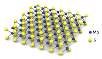
Crystal structure of molybdenum disulfideLayered structure of molybdenum disulfide (molybdenite, MoS2).[1]

(Via arXiv Preprint Server).

Electrical engineers at the Laboratory of Nanoscale Electronics and Structures of the Ecole Polytechnique Fédérale de Lausanne (Lausanne, Switzerland) have created the first molybdenite microchips. The chips had two to six transistors, and they were wired to perform some simple digital logic operations.[3] They were able to produce inverters and NOR gates operable at room temperature.[2-3] They reported on their devices in ACS Nano.[2,4]

The
Swiss engineers had investigated the bulk electrical properties of molybdenite, a naturally occurring mineral that's relatively abundant, earlier in the year. Its being a crystallographic analog of graphene, combined with its suitable semiconducting properties, encouraged further work. One advantage that molybdenite has over silicon is that it functions as a semiconductor in layers just three atoms thick.[3]

Transistors made of molybdenite have more gain than those fabricated from graphene.[3] Molybdenite also has mechanical properties that allow its use in flexible circuitry. I've never really seen the need for "roll-up" devices, but if they become poular, molybdenite can be used to make them. Molybdenite transistors would be useful for wearable electronics.[3]
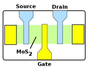
Molybdenite FETWhat could be simpler?

A molybdenite FET.

(Illustrated using Inkscape).
In a companion article in ACS Nano, the Swiss research team reported on the mechanical properties of molybdenite. Using techniques borrowed from graphene research, they exfoliated molybdenite layers and placed them over microfabricated circular holes in a silicon wafer. They were able to deform these few atomic layer membranes with an
atomic force microscope.[4]

The in-plane
stiffness of a MoS2 monolayer is 180±60 N/m. This value translates to a Young's modulus of 270±100 GPa, which is about the same as steel. As can be expected for a defect-free crystalline material, these membranes sustained strains of 6-11% before breaking. The average breaking stength was 23 GPa.[4]

One possible advantage that atomic layer semiconductors, such as graphene and molybdenite, may have in practical applications is that
short channel field effect transistors fabricated on thin layers are expected to have better properties than those made from other materials.[2]

References:

  1. M.M. Benameur, B. Radisavljevic, S. Sahoo, H. Berger and A. Kis, "Visibility of dichalcogenide nanolayers," arXiv Preprint Server, June 5, 2010.
  2. Branimir Radisavljevic, Michael Brian Whitwick and Andras Kis, "Integrated Circuits and Logic Operations Based on Single-Layer MoS2," ACS Nano, Article ASAP, November 10, 2011.
  3. Sarah Perrin, "First Molybdenite Microchip," Ecole Polytechnique Fédérale de Lausanne Press Release, December 5, 2011.
  4. Simone Bertolazzi, Jacopo Brivio and Andras Kis, "Stretching and Breaking of Ultrathin MoS2," ACS Nano, Article ASAP, November 16, 2011.